Thursday, July 27, 2006

Intel Launches Core2 Duo

Intel officially announced the introduction of 10 Core 2 Duo and Core Extreme microprocessors for desktops, workstations and notebooks. Intel said it has over 550 customer system designs underway, with the CPUs built on 65 nanometre technology. Machines using the desktop chips will be available in early August, while notebooks will become available at the end of that month.

Five of the family are aimed for desktops, five for notebook and mobile users. The products were formally codenamed "Cointreau" and "Merom". The chips support 64-32 instructions, so called smart cache which shares L2 cache, wide dynamic execution, and instructions that speed up multimedia transactions. The mobile chips have a better version of Speedstep, a method for powering down the processor to increase battery life, and other power saving devices.

Conroe chip is about 40% faster than the Pentium D while consuming 40% less power. The Merom chips are about 20% faster than the older Core Duo laptop chips at the same power level. The "Cointreau" chips clock from 2.93GHz down to 1.86GHz, all using a 1066MHz system bus, and with L2 caches of 4MB for the higher clocked chips and 2MB for the lower clocked chips. The "Merom" chips clock from 2.33GHz down to 1.66GHz with bus speeds of 667MHz and cache of either 4MB or 2MB for the two lowest SKUs (stock keeping units).

Intel has established the price for the desktop processors from about $180 to $1000 for 1,000-unit quantities. However, the price for the notebook processors remains to be specified at the end of August.


Monday, July 17, 2006

HP's Grain-size Wireless Chip

Today HP has announced the development of a miniature wireless chip small enough to embed in almost any object. The experimental chip has been developed by the "Memory Spot" research team at HP Labs in Bristol, England and is based on the CMOS (complementary metal oxide semiconductor) standard. This is a widely used type of semiconductor but has been shrunk by HP so it's just 2mm to 4mm square in size -- equivalent to a grain of rice.

The new chip has a 10 Mbps data transfer rate which is superior to both RFID tags and Bluetooth and is comparable to Wi-Fi speeds. It offers storage capacity ranging from 256 kilobits to 4 megabits in working prototypes, although future versions could have larger capacities. Information on the chip can be accessed by a read-write device that could be incorporated into a mobile phone, Personal Digital Assistant (PDA), camera or printer.

To access information, the read-write device is swiped over the chip, which is then powered-up so that the stored data is transferred instantly to the display of a device or printed out by the printer. Users could also potentially add information to the chip from their mobile devices. The miniature chip incorporates a built-in antenna and doesn't require a battery. It receives power through inductive coupling, which is the transfer of energy from one circuit component to another through a shared electromagnetic field, via a special read-write device, which can then extract content from the memory on the chip.

Some of the potential consumer and business-based applications that the chip could be used for include storing medical records on a hospital patient's wristband, or providing audio-visual extras such as music and commentary to digital postcards and photos. HP also believes that new applications could be developed which would help fight counterfeiting by adding added security to identity cards and passports. The Memory Spots could also supply additional information to any printed documents.

HP estimates that the miniature chip will be commercially available in about 2 years but believes there may soon be a time when they are obtainable in a booklet of self-adhesive dots, since these chips are easy to make.


Monday, July 10, 2006

First Commercial MRAM

Micrograph of the MR2A16A MRAM device

Freescale Semiconductor, which was spun-off from Motorola in 2004, has produced the first commercial non-volatile RAM product that can compete with normal RAM for speed and endurance but maintain its memory when the power is switched off. Austin, TX based Freescale announced the first commercial Magnetoresistive Random Access Memory (MRAM) device is now in volume production.

Potentially, MRAM could make all other forms of memory and storage obsolete, including normal RAM, Flash and magnetic storage.MRAM uses ferromagnetic material to store data and therefore doesn't rely on power like standard RAM to keep data stored. It consists of arrays of magnetic memory cells in which the information is stored as the magnetization direction of tiny ferromagnetic elements. It has the speed of ordinary volatile RAM without the need for power.

Unlike slower Flash RAM, which also doesn't need power to maintain storage, MRAM can be reliably written to, erased and overwritten almost indefinitively.According to Freescale, its 4 Mbit MRAM product is a fast, non-volatile memory with unlimited endurance. Freescale's successful commercialization of MRAM technology could hasten new classes of electronic products offering dramatic advances in size, cost, power consumption and system performance. Companies like Toshiba, NEC and IBM have announced continued research and breakthroughs in MRAM technology, but Freescale is the first to announce commercial availability of the product.

Freescale's first commercial MRAM product, called the MR2A16A, has a variety of applications. Sometimes referred to as "universal" memory, MRAM could displace a number of chips found in every electronic device, from PCs, cell phones, music players and cameras to the computing components of kitchen appliances, cars and airplanes. According to Freescale, the product is engineered to be a replacement for battery-backed SRAM units. It also could be used in cache buffers, configuration storage memories and other applications that require the speed, endurance and non-volatility of MRAM.


Monday, July 03, 2006

Top500 Supercomputers

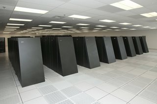
BlueGene/L system, No.1 Supercomputer
[Photo courtsey: Lawrence Livermore National Laboratory (LLNL)]


Last week the 27th edition of the TOP500 list of the world's fastest supercomputers was released at the International Supercomputing Conference held in Dresden, Germany.

The top spot was occupied by the BlueGene/L system, developed jointly by IBM and DOE's National Nuclear Security Administration (NNSA), and installed at DOE's Lawrence Livermore National Laboratory in California. BlueGene/L has occupied the number one position of the last three TOP500 lists. It has reached a performance speed of 280.6Teraflops (trillions of calculations per second) and is still the only system ever to exceed 100Teraflops.

The list is dominated by IBM with 48.6% of the 500 systems listed, and 4 of the top 10, supplied by the company. Processors from Intel power more than 300 of the supercomputers in the TOP500.

One sad note before we end this posting. Sandia's ASCI Red supercomputer, a stalwart of the TOP500 for an unprecedented nine years, is being decommissioned. ASCI Red was the first computer to reach 1Teraflop performance in 1996, and was rated as the fastest computer in the world for four years. During its operation the NNSA used ASCI Red for its advanced simulation and computing research programme, helping to evaluate the safety of America's nuclear arsenal.